
Loading...
MTI | SKU:
GEsba50D045C2R0001US
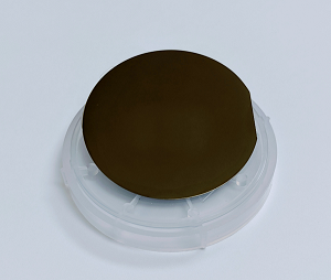
Ge Wafer (100) 2" dia x 0.45 mm, 2SP, N type (Sb doped), resistivities: 0.001-0.01 ohm-cm
€0,00
Unit price
/
Unavailable
Couldn't load pickup availability
Delivery and Shipping to EU
Delivery and Shipping to EU
We will add in the quotation, the shipping, insurance, customs clearance costs.

Ge Wafer (100) 2" dia x 0.45 mm, 2SP, N type (Sb doped), resis...
€0,00
Unit price
/
Unavailable
Ge Wafer (100) 2" dia x 0.45 mm, 2SP, N type (Sb doped), resistivities: 0.001-0.01 ohm-cm
MTI
Ge Wafer Specification
- Growing Method: CZ
- Orientation: (100) +/_0.5 Deg.
- Wafer Size: 2" dia x 450 microns
- Surface Polishing: Two sides epi polished
- Surface roughness: RMS or Ra:~ 10 A ( by AFM)
- Doping: Sb Doped
- Conductor type: N-type
- Resistivity: 0.001-0.01 Ohms/cm (If you would like to measure the resistivity accurately,
please order our Portable 4 Probe Resistivity Testing Instrument.) - Package: under 1000 class clean room
Typical Properties:
- Structure: Cubic, a = 5.6754 A
- Density: 5.323 g/cm3 at room temperature
- Melting Point: 937.4 oC
- Thermal Conductivity: 640
Related Product
|
|
|
|
|