GaN Template on Sapphire (0001), N type, undoped, 2"x 0.5mm,1sp GaN Film:30um, (Production Grade) - FmGaNonALC50D05C1FT30um
Couldn't load pickup availability
Delivery and Shipping to EU
Delivery and Shipping to EU
We will add in the quotation, the shipping, insurance, customs clearance costs.
GaN Template on Sapphire (0001), N type, undoped, 2"x 0.5mm,1sp GaN Film:30um, (Production Grade) - FmGaNonALC50D05C1FT30um
MTI
-GaN Template on saphhire is made by a hydride vapor phase epitaxy (HVPE)-based method. During the HVPE process, HCl reacts with molten Ga to form GaCl, which in turn reacts with NH3 to form GaN. GaN template is a cost effective way to replace GaN single crystal substrate.
Specifications:
Production grade
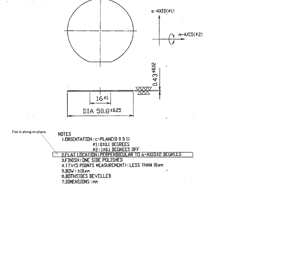
- Sizes 2” Round
- Dimensions 50.8mm +/- 0.25mm
- Substrate Sapphire, C-plane-(0001) with 0.2 degree miscut toward M-plane
- Conduction Type: N-type,
- Resistivity :N/A
- Front Surface Finish (Ga Face) As-grown
- Back Surface Finish Sapphire as-received finish
- Useable Surface Area >90%
- Edge Exclusion Area 1mm
- Package Single Wafer Container
- GaN layer thickness : 30 microns , (+/- 10%) with roughness: ~10 nm RMS as measured by the Wyko (white light interferometer) for 50 umx50um area
Macro Defect Density: <=5 cm^-2
Lattice Constant Mismatch: 14% mismatch
Dislocation Density: 5x10^9/ cm^2
Related data
- Please click here to see XRD Rocking curve of GaN template
- Please click here to see Dislocation vs Thickness of GaN template
- Please click here to see RMS of GaN template
Related Products
 |
|||||


