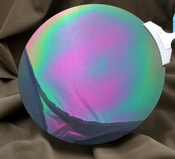
GaN Template on 2" Silicon Wafer, GaN film(500nm), N type, undoped on Si (111) substrates, 2"x 0.279 mm, 1sp
Couldn't load pickup availability
Delivery and Shipping to EU
Delivery and Shipping to EU
We will add in the quotation, the shipping, insurance, customs clearance costs.
GaN Template on 2" Silicon Wafer, GaN film(500nm), N type, undoped on Si (111) substrates, 2"x 0.279 mm, 1sp
MTI
GaN Template on silicon is made by a hydride vapor phase epitaxy (HVPE)-based method. During the HVPE process, HCl reacts with molten Ga to form GaCl, which in turn reacts with NH3 to form GaN. GaN template on silicon is a cost effective way to replace GaN single crystal substrate.
- Research Grade , about 90 % useful area
- Nominal GaN thickness: 0.5?m ± 0.1 ?m
- Front Surface finish (Ga-face): <1nm RMS, As-grown
- Back surface finish: as received
- GaN orientation: C-plane (00.1)
- Polarity: Ga-face
- Conduction Type: Undoped (N-)
- Macro Defect Density: <5/cm^2
- Wafer base: Silicon [111], N type, P doped, Res: 1-10 ohm-cm, 2" diameter x 0.279mm, one side polished
- There is ~200nm AlN buffer layer between the silicon and GaN
Related data
- Please click here to see XRD Rocking curve of GaN template
- Please click here to see Dislocation vs Thickness of GaN template
Related Products
 |
|||||


