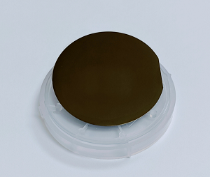
GaAs Wafer , Growing Method: VGF, (100) undoped Semi-Insulated 3"D x0.5 mm, 1SP
Couldn't load pickup availability
Delivery and Shipping to EU
Delivery and Shipping to EU
We will add in the quotation, the shipping, insurance, customs clearance costs.
GaAs Wafer , Growing Method: VGF, (100) undoped Semi-Insulated 3"D x0.5 mm, 1SP
MTI
GaAs single crystal wafer
Growing Method: VGF
Orientation: (100)
Size: 3" dia x 0.5mm
Polishing: one side polished
Doping: undoped
Conductor type: Semi-Insulating
Resistivity: (1.35-4.21)x10^8Ohm.cm
Mobility: 4360-5640cm^2/V.S
EPD: <5000cm^-2
Primary Flat: EJ(0-1-1)
Secondary Flat: EJ(0-11)
Ra(Average Roughness) : < 0.4 nm
Related Products
| Other GaAs |
InSb |
Other InAs |
InP |
GaSb |
Wafer Box |
Film Coater |
RTP Furnaces |


